| Sign In | Join Free | My carsrow.com |
|
- Home
- Products
- About Us
- Quality Control
- Contact Us
- Get Quotations
| Sign In | Join Free | My carsrow.com |
|
Brand Name : OEM
Model Number : Customized
Certification : ISO9001/ISO14001
Place of Origin : Guangdong China
MOQ : 5pcs
Price : negotiable
Payment Terms : T/T
Supply Ability : 10000pcs per month
Delivery Time : 10-14 wds
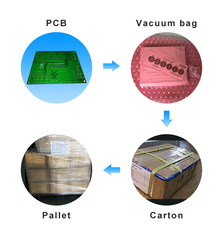
Packaging Details : 25 sets in Vacuum bag/ Carton
Material : High TG FR4
Layers : 2-48 layers
Max size : 610X915mm
Min Via : 0.1mm
Surface treatment : ENIG
Color : Matt Green
Board thickness : 0.15-4.5mm
Outer layer copper thickness : 1/3-12OZ
High TG170 FR4 Multilayer HDI PCB with Buried and Blind Via Holes
1. Product Descprition
| Item | Specification |
| Material | High TG FR4 |
| Layers | 4-20 layers |
| HDI | HDI plus 1 or 2 |
| Copper thickness | 1/3-12OZ |
| Minimum Via | 0.1mm |
| Surface treatment | ENIG,OSP |
| Board thickness | 0.15-4.5mm |
| Solder mask color | Gree,Blue,Black,Red,White |
| Tolerance of board thickness | T>=1.0mm, Tol: +/-10% T<1.0mm, Tol:+/-0.1mm |
2.HDI capablity and example
1) X+X process

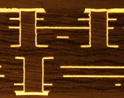
( Layer Drawing) (Cross section)
2) 1-N-1 process


( Layer Drawing) (Cross section)
3)2-N-2 process-B
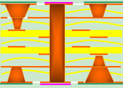
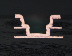
( Layer Drawing) (Cross section)
4)2-N-2 process-N(Advanced:6+N+6)
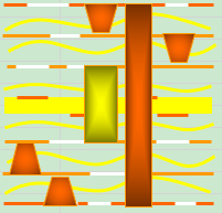
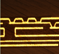
( Layer Drawing) (Cross section)
3. Application
1)Communication electronic equipment:Smartphone,Multifunctional Phone,visual telephone
2)Computer:Laptop, Super computer, Pad.
3) Consumer Electronics: Camera, Digital TV, Video
4) Car
5) Equipments
6) Space and aviation: satellite,guided missile
7) Medical Appliances
8) Industral Control
4.Package
|
|
High TG170 FR4 Multilayer HDI PCB Board Buried and Blind Via Holes Images |